The quality and dependability of microchips are crucially dependent on test wafers, which are frequently disregarded in the semiconductor production process. These tiny, spherical silicon discs are an essential tool for semiconductor producers all over the world since they serve as the basis for testing and certifying the production process.
Despite their significance, working with test wafers presents unique challenges. Understanding these challenges is crucial for optimizing the testing process and ultimately improving product quality. In this blog post, we’ll delve into the world of test wafers, exploring materials, equipment, best practices, and troubleshooting techniques to help you navigate this critical aspect of semiconductor manufacturing.
In This Post
Understanding Test Wafer Materials and Types
Test wafers come in various materials, including silicon, gallium arsenide, silicon carbide, and even specialized options like Patterned Silicon Wafers. The choice of material depends on the specific application, as each material offers distinct advantages and disadvantages. Silicon wafers are popular due to their affordability and widespread availability, making them ideal for many testing scenarios.
Gallium arsenide and silicon carbide, on the other hand, excel in high-frequency and high-temperature applications. These options, including Short Loop Wafers, cater to diverse industry needs, ensuring the right material is available for every testing requirement.
Furthermore, they can vary in terms of size and thickness, with diameters typically ranging from 100mm to 300mm. It’s essential to select the right material and size to match your testing needs accurately. Consult with your semiconductor supplier or engineer to make an informed choice.
Selecting the Right Test Wafer for Your Application
Choosing the appropriate one is a critical decision that directly impacts the accuracy and reliability of your testing. To make an informed choice, consider factors such as the material’s electrical properties, thermal conductivity, and mechanical strength. Additionally, assess the compatibility of it with your testing equipment and procedures.
For example, if you’re testing high-frequency devices, gallium arsenide wafers might be the preferred choice due to their excellent RF performance. However, silicon wafers are more suitable for general-purpose testing due to their affordability and compatibility with standard testing equipment.
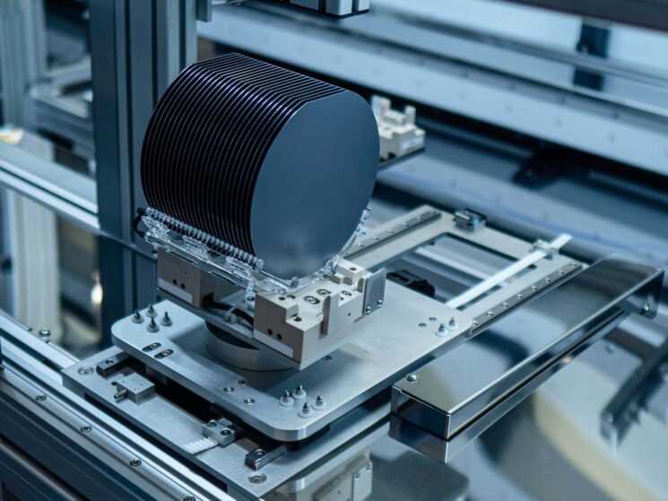
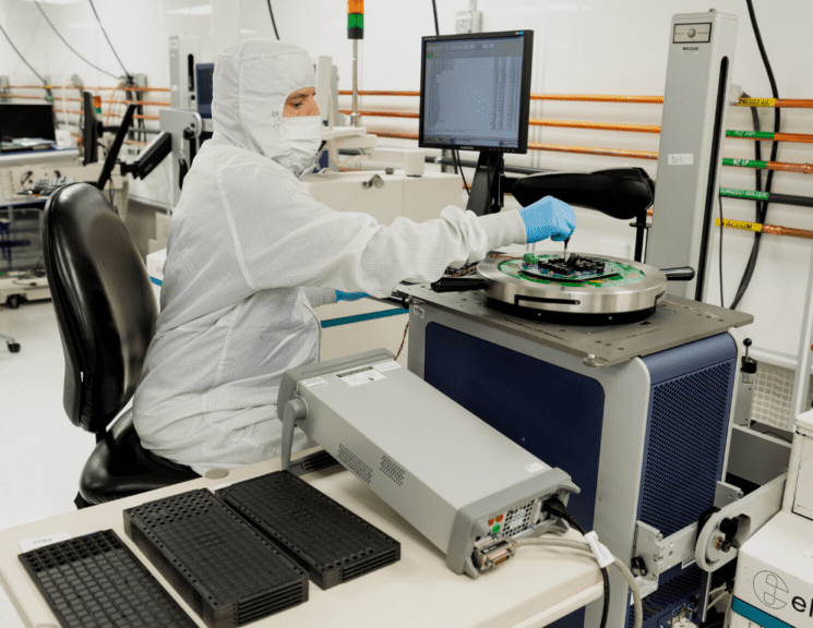
Essential Equipment for Handling
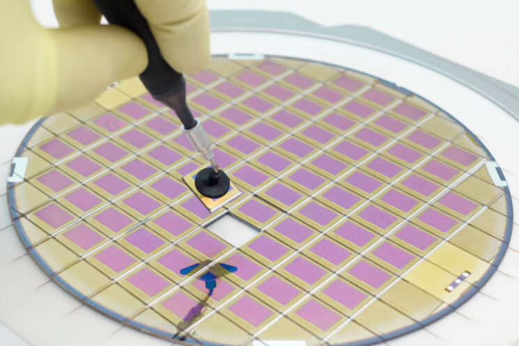
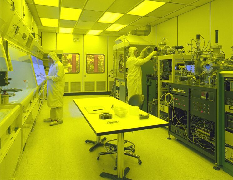
Handling them demands precision and care, and having the right equipment is non-negotiable. Cleanrooms, equipped with controlled temperature and humidity, provide the foundational environment for preserving wafer integrity. Essential tools include specialized tweezers, vacuum wands, and wafer carriers, ensuring gentle and precise handling while minimizing contamination risks.
Additionally, wafer inspection microscopes enable close examination for defects or contaminants before and after testing. Proper storage is equally vital, achieved through wafer storage cabinets that maintain a controlled environment to shield wafers from dust, moisture, and other pollutants. These pieces of equipment, when employed meticulously, safeguard and guarantee the reliability of semiconductor testing processes.
Best Practices for Storage and Handling
Storing and handling them demand rigorous adherence to best practices. Wafers should always be stored in individual carriers to prevent damage from contact with other wafers. Furthermore, maintaining a clean and organized storage area with clearly labeled wafers ensures easy retrieval and minimizes handling errors.
When handling wafers, avoid direct contact with bare hands, as skin oils and particles can contaminate the surface. Always use cleanroom gloves or handling tools. Additionally, establish a strict protocol for handling, including inspection before and after each use to detect any damage or contamination.
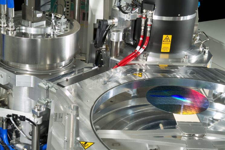
Cleaning and Preparing for Testing
Cleaning and preparing them before testing is a crucial step to ensure accurate results. Use a combination of ultrasonic cleaning and chemical processes to remove particles, residues, and organic contaminants. Always follow the recommended cleaning procedures provided by your supplier or equipment manufacturer.
Once cleaned, wafers should undergo a thorough inspection to confirm their readiness for testing. Any defects or remaining contaminants can significantly impact test results and compromise product quality.
Avoiding Common Contamination Issues
Contamination is a persistent challenge in semiconductor manufacturing. Common contaminants include particles, chemical residues, and even airborne molecular contaminants (AMCs). To mitigate contamination issues, follow these strategies:
- Regular Cleanroom Maintenance: Keep cleanrooms clean and well-maintained to minimize particle generation.
- Use of Particle Filters: Install HEPA and ULPA filters to capture particles from the air.
- Chemical Management: Monitor and control the use of chemicals to prevent cross-contamination.
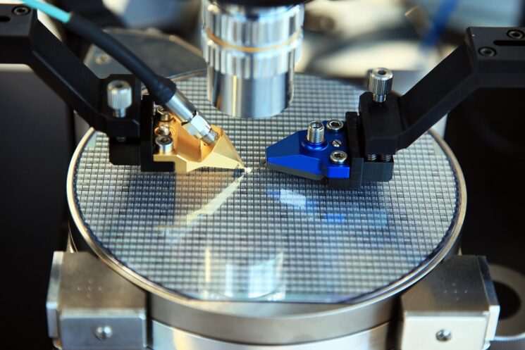
Effective Testing Strategies
When it comes to testing strategies, there is no one-size-fits-all approach. Your testing methods should align with your specific goals and the properties of the themes you’re working with. Consider the following strategies:
- Parametric Testing: Measure specific electrical characteristics, such as voltage, current, and resistance, to ensure the wafers meet specifications.
- Functional Testing: Evaluate the overall performance of semiconductor devices, assessing their functionality in real-world scenarios.
- Reliability Testing: Expose wafers to accelerated aging conditions to predict their long-term performance and reliability.
- Failure Analysis: Investigate wafers that fail during testing to identify root causes and improve the manufacturing process.
Analyzing Test Wafer Data and Results
Collecting data during testing is only half the battle. Effective analysis of the data is essential for making informed decisions and optimizing the manufacturing process. Implement statistical analysis and data visualization techniques to identify trends, anomalies, and potential areas for improvement. Collaborate with data analysts and engineers to extract meaningful insights from your data.
Troubleshooting Test Wafer-related Problems
Despite meticulous planning, issues may arise during the process. Common problems include equipment malfunctions, contamination, and unexpected deviations in examination results. Establish a troubleshooting protocol that includes clear steps for identifying, isolating, and resolving these issues promptly. Regular training and communication among team members are also essential for addressing problems effectively.
Conclusion: Optimizing Test Wafer Processes for Success
Navigating the world can be challenging, but with the right knowledge and practices, you can streamline your semiconductor manufacturing process and enhance product quality. Selecting the appropriate materials, using the right equipment, and adhering to best practices in storage, handling, and testing are key to success.
Remember that continuous improvement is essential in the semiconductor industry. Regularly review and refine your processes, stay up-to-date with the latest technologies, and collaborate with experts in the field to ensure you’re always at the forefront of semiconductor manufacturing excellence. By following these tips and tricks, you’ll be well on your way to mastering the art of navigation and achieving success in your semiconductor endeavors.